
The short answer
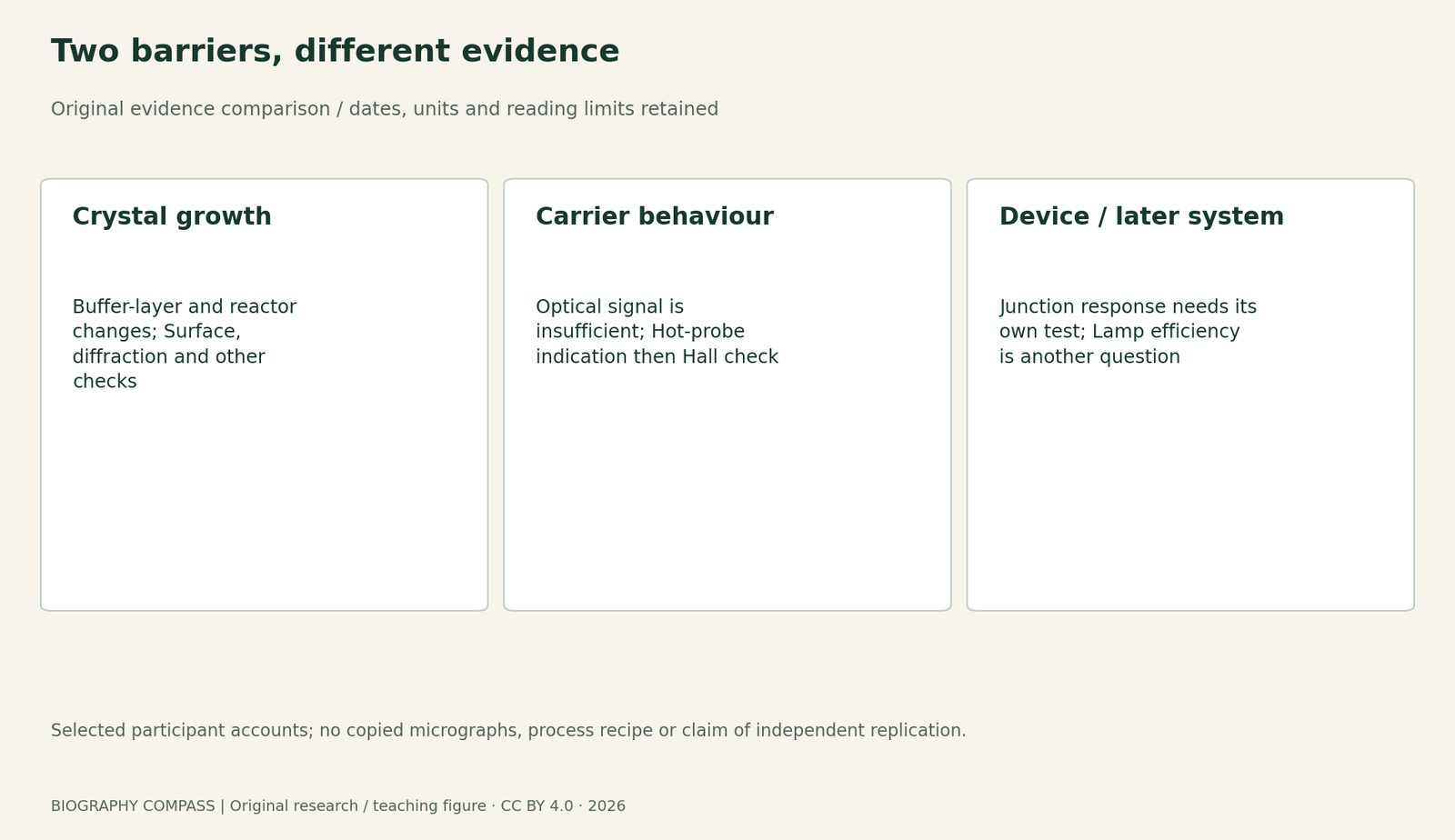
A smooth semiconductor film is not automatically a working light-emitting junction. Akasaki and Amano’s accounts describe different obstacles in gallium nitride: growing useful crystals and obtaining the required electrical behaviour. Keeping the evidence for each stage separate explains the advance more clearly.
Original source comparison
Which measurement answers which question?
A stronger result in one column cannot substitute for a missing result in another.
| Country | What the evidence supports | What it does not establish |
|---|---|---|
| Surface / crystal checks | Whether specified material properties improved | The sign of the dominant electrical carrier |
| Emission measurement | What light was detected under stated conditions | P-type conduction by itself |
| Carrier and junction tests | Specified electrical and device behaviour | All later lighting-system performance |
Chronology
A timeline of the turning points
Buffer-layer progress
Growth quality improved before all device barriers were removed.
Mg-doped p-type work
Carrier measurements answered an electrical question.
Thermal-annealing publication context
A separate treatment route appears in the lecture’s chronology.
Shared recognition
The prize joins contributions from distinct research programmes.
The buffer-layer advance had several kinds of evidence
Akasaki’s printed pages 15–18 describe reactor changes, contributions by Yasuo Koide and Hiroshi Amano, and low-temperature buffer-layer work developed in 1985. The thin AlN layer preceded further GaN growth on sapphire. Surface appearance was one check. The account also discusses microscopy, diffraction, electrical properties and luminescence as evidence that the material improved. Those observations answer related questions about crystal quality; they are not interchangeable measurements. A transparent or mirror-like surface was encouraging, but the physical interpretation rested on more than the attractive appearance of one specimen. No historical micrograph is reproduced in this guide.
Sources for this section: [1]
A brighter zinc-doped sample was not the required result
Amano’s printed pages 47–49 distinguish optical observations from p-type conduction. Low-energy electron-beam treatment enhanced emission in zinc-doped material without producing the desired electrical behaviour. Magnesium-doped samples then supplied a different line of investigation. This distinction prevents a common shortcut in technology histories: one visible improvement becomes shorthand for solving every remaining problem. An emission spectrum and a conductivity test concern different properties. Their results can contribute to one development programme without one result proving the other. The historical treatment sequence is discussed here as evidence, not as operating instructions for semiconductor processing.
Sources for this section: [2]
The account distinguishes a preliminary check from a stronger one
Amano recalls that treated Mg-doped samples suggested p-type behaviour in a hot-probe test. He regarded that indication as insufficiently convincing and credits Mr Kito with Hall-effect measurements that strengthened the identification. The lecture then describes fabrication of junction devices. It separately discusses Nakamura’s later thermal-annealing route. Amano’s autobiographical recollection uses 1991 for that work, while his lecture discusses the 1992 claim and paper. Retain the type of date and the source rather than forcing experimental recollection and publication into one undifferentiated year. The laboratories and treatment routes also remain distinct.
Original worksheet: diagnose three overstatements
Consider three invented evidence cards. Card A records a smoother surface and narrower diffraction feature after a buffer-layer change. Card B records stronger light emission after treatment, with no carrier-sign measurement supplied. Card C records a specified carrier measurement consistent with p-type conduction and a separately tested junction response. Match each card to the narrowest supported claim. Evaluate these statements: A proves a finished blue LED; B proves p-type conduction; C proves every commercial white lamp will be efficient. Identify the extra evidence needed for each wider claim. The cards are teaching summaries, not digitised results from the original experiments.
Reference answers preserve the contribution of each stage
A supports improved material quality under the stated checks, not a complete device. B supports increased emission under its measurement conditions, not identification of the majority carrier. C supports the specified electrical and junction findings, not the performance of every later lighting system. Device colour, output, reliability and efficiency require their own measurements, while a white-light product adds further components and losses. The 2014 prize shared by Akasaki, Amano and Nakamura recognises connected contributions without making them one identical experiment. A useful historical account follows the progression from a growth problem to material checks, carrier evidence and device tests, keeping both collaborators and uncertainty visible.
Continue the chronology
Related history guides
Chalfie’s Worm Research: Anatomy, Expression and Function
Compare a different measurement question and its explicitly bounded worked exercise.
Read the timeline1985 calcium-indicator paperTsien’s Calcium Indicators: Why a Ratio Needs Calibration
Compare a different measurement question and its explicitly bounded worked exercise.
Read the timelineBiography context
Explore Japan through connected lives
Isamu Akasaki
Read the cited career account and named research contributions.
Explore the biographiesBiographyHiroshi Amano
Read the cited career account and named research contributions.
Explore the biographiesBiographyShuji Nakamura
Read the cited career account and named research contributions.
Explore the biographiesConnected biographies
People behind the work
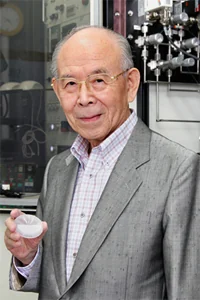
1929–2021
Isamu Akasaki
Semiconductor physicist and university researcherIsamu Akasaki was a Japanese researcher who pursued gallium nitride as a material for short-wavelength light emitters. Work with students and colleagues on crystal growth and p-type conduction helped establish a route toward efficient blue LEDs.Read biography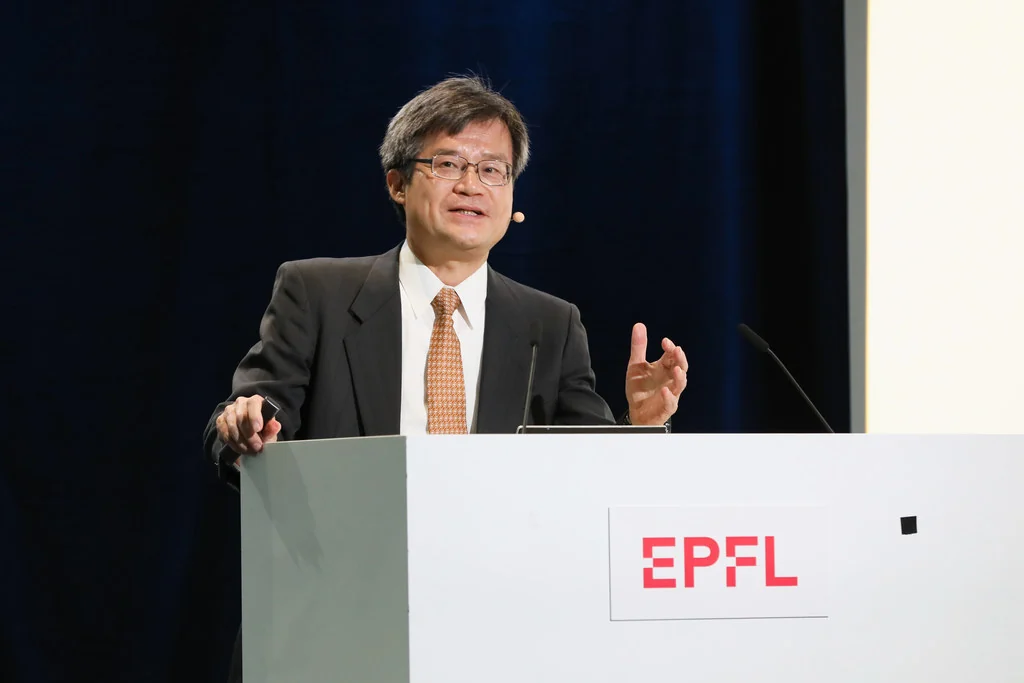
Born 1960
Hiroshi Amano
Electronic engineer and nitride-semiconductor researcherHiroshi Amano is a Japanese engineer whose work in Isamu Akasaki’s laboratory helped overcome barriers in gallium-nitride light emitters. His research on buffer layers and p-type GaN contributed to the 2014 Nobel Prize in Physics.Read biography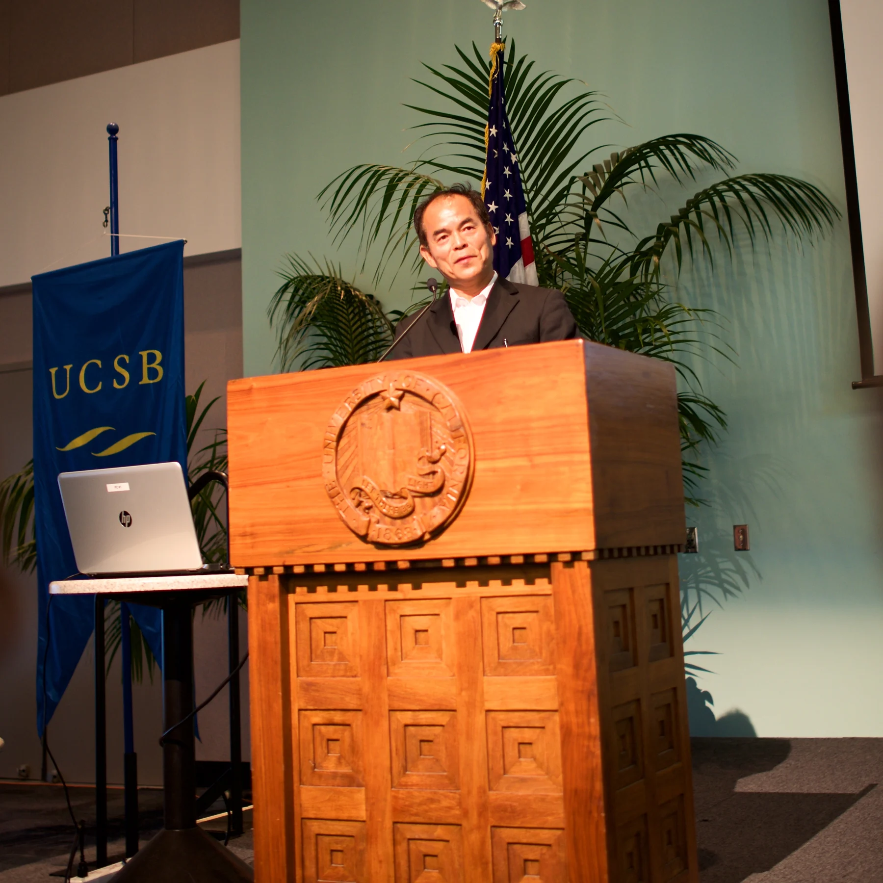
Born 1954
Shuji Nakamura
Electronic engineer and semiconductor researcherShuji Nakamura is a Japanese-born engineer whose work at Nichia helped make efficient blue LEDs practical. His research on difficult semiconductor materials contributed to the 2014 Nobel Prize in Physics and later continued at the University of California, Santa Barbara.Read biographyQuick answers
Common questions
- Did electron-beam-enhanced zinc emission establish p-type GaN?
- Amano’s account explicitly distinguishes the enhanced optical signal from obtaining p-type conduction.
- Does this guide provide a fabrication recipe?
- No. It compares the evidential role of historical measurements without giving an operating protocol.
Primary and institutional sources
How this history was checked
Compare the identified original texts, participant accounts and institutional records; the teaching examples are separately labelled. This article was reviewed on 27 October 2026.
- Isamu Akasaki; Nobel FoundationFascinated Journeys into Blue Light,8 December 2014,7–37
- Hiroshi Amano; Nobel FoundationGrowth of GaN on Sapphire via Low-Temperature Deposited Buffer Layer and Realization of p-Type GaN by Mg Doping Followed by Low-Energy Electron Beam Irradiation,8 December 2014,43–53
- Hiroshi Amano; Nobel FoundationHiroshi Amano: autobiographical account,2014
- Nobel FoundationIsamu Akasaki: prize facts
- Nobel FoundationHiroshi Amano: prize facts