
The short answer
How can a charge-coupled device transfer and read an image?
Compare the evidence
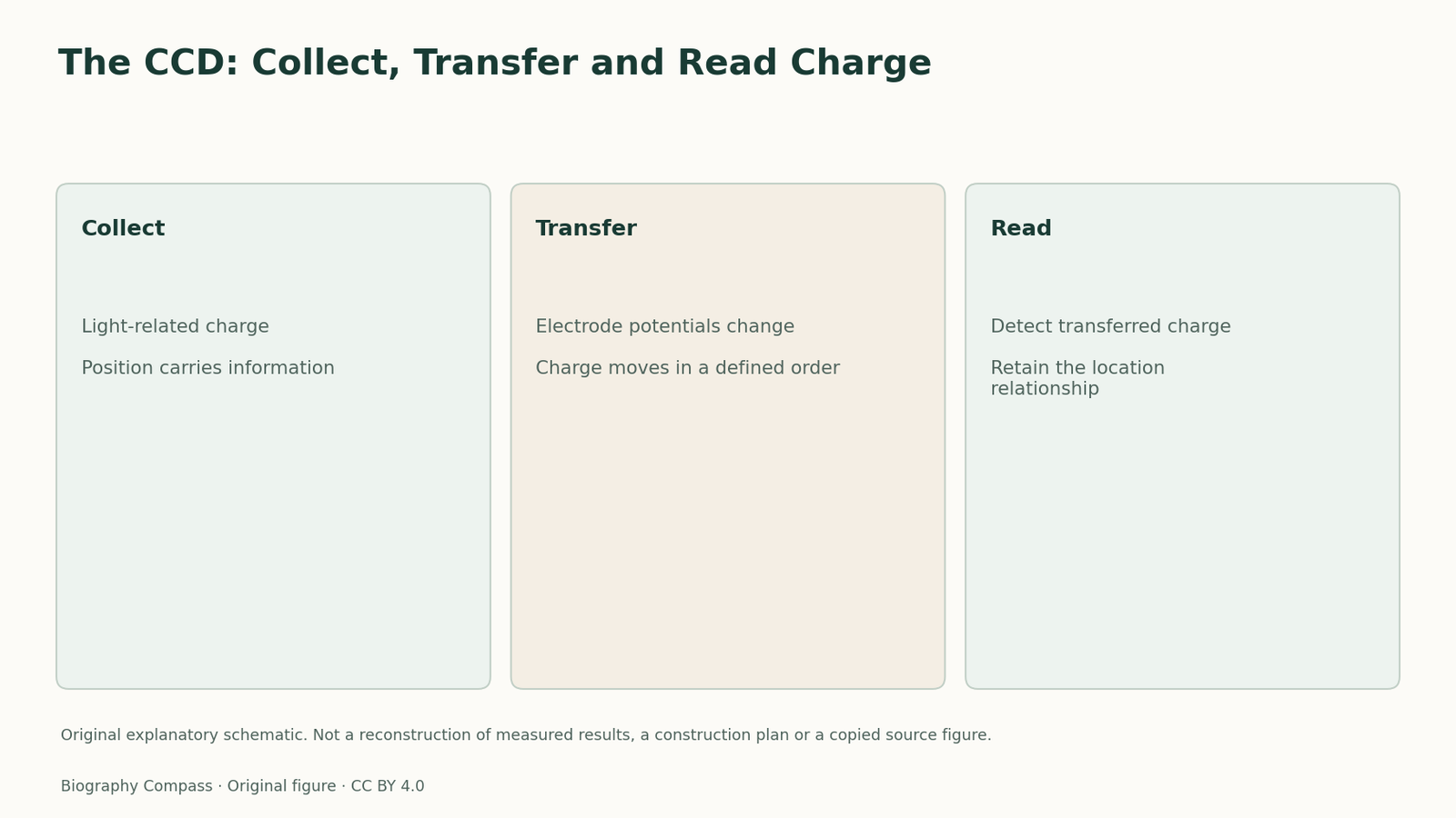
The CCD: Collect, Transfer and Read Charge
Compare what each inspected record establishes with the claim that remains separate.
| Record or observation | What it supports | What remains separate |
|---|---|---|
| 1970 device concept paper | Separates stored charge, controlled transfer and detection | Does not describe literal buckets physically moving across a chip |
| Official award and career records | Connect the principle with Smith, Boyle and imaging history | Do not make every current camera a CCD or erase later contributors |
An image and a readout sequence are different representations
A CCD image sensor can collect light-generated charge at many positions, preserving information about how illumination varied across its surface. Reading that information requires moving and detecting charge in an organised way. Boyle and Smith's 1970 paper sets out the broader device principle: charge is stored in potential wells, transferred through changes in electrode potentials and detected. Imaging was one of the applications considered, rather than the only possible use of charge transfer.
The electrodes control the transfer
The concept does not involve tiny solid buckets physically travelling across a chip. Voltages change the potential arrangement so that stored charge can move to a neighbouring location. Smith's later technical account places this principle in the history of semiconductor devices and memory ideas. Collection, transfer and detection therefore need separate labels in an explanatory diagram. A failure in one stage should not automatically be described as a failure in every part of an imaging system.
Preserve position through an invented sequence
For an original classroom model, give four numbered locations invented charge counts of one, three, zero and two. Move the counts in a specified order to one readout location while keeping their original position numbers. Ask what is lost if the order is forgotten. The answer is the relationship between signal and location, even if the total charge remains the same. This invented sequence illustrates ordering without modelling transfer losses or reproducing historical measurements. They illustrate why an image sensor needs an organised path from collected information to a reconstructable output.
Continue the chronology
Related history guides
Biography context
Explore United States through connected lives
Connected biographies
People behind the records

1930–2025
George E. Smith
Applied physicist and semiconductor-device researcherInvention of the charge-coupled device with Willard Boyle.Read biography1926–2018
Jun-ichi Nishizawa
Semiconductor engineer and university presidentPIN-junction and static-induction-device research and contributions to optical communications.Read biography
1899–1990
Kenjiro Takayanagi
Television engineer, researcher and educatorA1926 television demonstration using mechanical scanning and a cathode-ray-tube display.Read biographyQuick answers
Common questions
- How can a charge-coupled device transfer and read an image?
- A CCD represents information as stored charge and shifts it through controlled potential changes to a readout. For imaging, the transfer order preserves the relationship between each signal and its original position.
Primary and institutional sources
How this history was checked
Sources distinguish individual patent or technical records from biographical and retrospective accounts. Their actual reading scope is retained in the biography source notes. This article was reviewed on 7 November 2026.
- Nobel Prize OutreachGeorge E.Smith—Facts
- George E.Smith / Nobel Foundation,2009George E.Smith—Biographical
- W.S.Boyle and G.E.Smith / Bell System Technical Journal,1970Charge Coupled Semiconductor Devices
- George E.Smith / Reviews of Modern Physics,2010Nobel Lecture:The invention and early history of the CCD