
The short answer
What does the intrinsic layer do in a PIN diode?
Compare the evidence
The PIN Layer: Collection and Capacitance
Compare what each inspected record establishes with the claim that remains separate.
| Record or observation | What it supports | What remains separate |
|---|---|---|
| Historical museum biography | Links Nishizawa with PIN-junction research | Does not supply the mechanism of every modern photodiode |
| Manufacturer’s PIN explanation | Separates collection, capacitance and ordinary unity-gain operation | Does not make improved speed proof of avalanche multiplication |
The middle region has a functional role
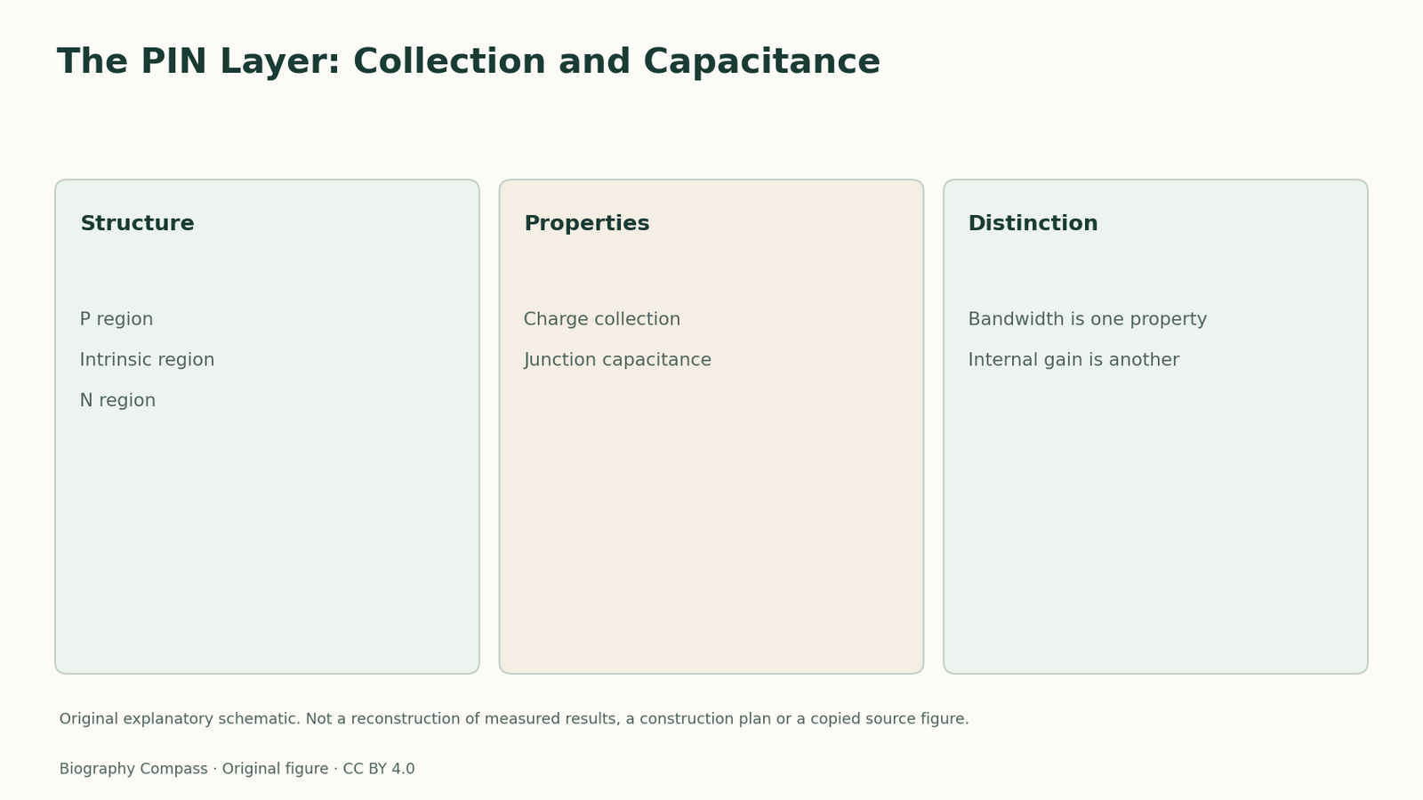
A PIN photodiode places an intrinsic region between the P and N regions. Hamamatsu's technical account explains that this arrangement can reduce capacitance per unit area and improve frequency response. The region is therefore not simply a spacer added to make a drawing longer. Its electrical properties and the depletion arrangement affect how the detector collects and reads a light-generated signal. Device structure and the external circuit together determine useful performance.
Sources for this section: [3]
Collection is different from internal multiplication
The same technical account distinguishes ordinary PN/PIN photodiodes from avalanche devices with internal gain. A PIN structure can improve collection and bandwidth without multiplying each initial carrier through an avalanche mechanism. This prevents a misleading shortcut in which every improvement in sensitivity or speed is described as amplification. Nishizawa's historical connection with PIN-junction work gives context, but the modern explanation should not be mislabelled as a reconstruction of one unexamined 1950s device.
Separate three measurement questions
For an original classroom exercise, draw boxes labelled charge collection, capacitance and internal gain. Place the PIN intrinsic-region discussion beside the first two and leave avalanche multiplication in a separate category. Ask whether a faster response proves that internal gain increased. It does not. The supported answer identifies which property was measured rather than substituting one favourable adjective for all of them. This schematic supplies no doping profile, layer thickness, voltage setting or detector recommendation. It is a method for reading device explanations, not a manufacturing specification or a quantitative performance claim.
Continue the chronology
Related history guides
Biography context
Explore Japan through connected lives
Connected biographies
People behind the records
1926–2018
Jun-ichi Nishizawa
Semiconductor engineer and university presidentPIN-junction and static-induction-device research and contributions to optical communications.Read biography
1930–2025
George E. Smith
Applied physicist and semiconductor-device researcherInvention of the charge-coupled device with Willard Boyle.Read biography
1886–1976
Hidetsugu Yagi
Telecommunications engineer and university leaderJoint directional-antenna work with Shintaro Uda and international communication of that research.Read biographyQuick answers
Common questions
- What does the intrinsic layer do in a PIN diode?
- The intrinsic region can reduce capacitance per area and improve response. Ordinary PIN operation does not include avalanche carrier multiplication, so collection and bandwidth improvements should not be called internal gain.
Primary and institutional sources
How this history was checked
Sources distinguish individual patent or technical records from biographical and retrospective accounts. Their actual reading scope is retained in the biography source notes. This article was reviewed on 7 November 2026.