
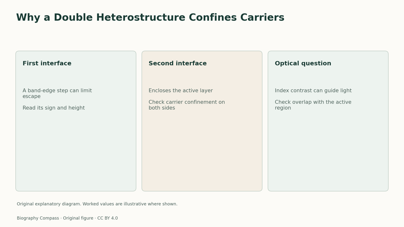
The short answer
What changes when an active semiconductor layer is placed between materials with different band edges?
Read the evidence
Two confinement mechanisms
The active region has carrier and optical requirements with different physical origins.
| Mechanism | Quantity that changes | Purpose |
|---|---|---|
| Carrier confinement | Band edges across interfaces | Keeps electrons or holes near the active region |
| Optical guidance | Refractive index across materials | Shapes the optical field |
| Gain and loss | Net light amplification | Determines whether the architecture works as a laser |
Compare the energies across an interface
A semiconductor has energy ranges in which electrons can occupy states. Put two different semiconductors together and their band edges may change across the interface. An electron that would need more energy to enter the adjacent material can spend more time in the lower-energy region. A double heterostructure uses two such interfaces around an active layer. With the appropriate alignment, electrons and holes can both be concentrated where light is to be generated. The precise offsets depend on the material combination. A larger band gap alone does not specify how the change is divided between the two band edges.
Why two sides matter
A single interface can impede motion in one direction. An active layer enclosed between barriers can reduce escape on both sides. This changes the distribution of carriers available to participate in recombination. In a laser, the useful question is whether enough carriers can accumulate in the active region for optical gain to exceed losses. Confinement can assist that condition, but it is not the only requirement. The device must still supply carriers, support an optical mode and manage losses. Kroemer’s architecture identifies a way to address the carrier distribution without making those other questions disappear.
An invented energy step
Suppose an electron in a classroom diagram sits in a region whose band edge is represented by zero units. The two adjoining layers have edges represented by plus three. A carrier with one unit above the central edge cannot cross either step classically without gaining energy. Raise only one adjoining edge and the other side would remain easier to leave. This is an illustrative comparison of two band profiles. It omits quantum tunnelling, temperature and actual band offsets, and the numbers are not instructions for constructing a device. Its purpose is to show what the two interfaces contribute separately.
Sources for this section: [2]
Read the proposal as a statement of feasibility
The 1963 contribution proposed an architecture and explained why it could address limitations of semiconductor injection lasers. Evidence that a later device operates includes additional information about actual materials and measured performance. The relationship between the records is instructive. The proposal sets out a mechanism, while later implementation tests whether its requirements can be met together. If a report discusses low threshold or continuous operation, ask what carrier confinement, optical loss and thermal conditions were measured. Those quantities connect the architecture to its observed result without treating a band diagram as a completed device.
Continue the chronology
Related history guides
Why Hopping Conduction Has a Quarter-Power Law
Read Mott’s low-temperature hopping argument and use an original example to see why electrons may favour a farther state with a smaller energy cost.
Read the timeline1977–1978How Modulation Doping Improved Electron Mobility
Read the 1978 carrier–donor separation study and compare electron density with mobility in an original example of semiconductor transport.
Read the timelineBiography context
Explore United States through connected lives
Connected biographies
Researchers and collaborators
1928–2024
Herbert Kroemer
Semiconductor physicist and engineerRead Herbert Kroemer’s path from Göttingen to RCA, Varian and UC Santa Barbara, including his proposal for a double-heterostructure semiconductor laser.Read biography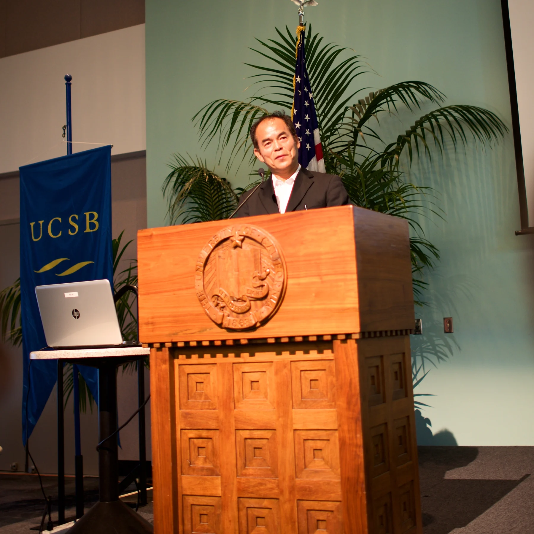
Born 1954
Shuji Nakamura
Electronic engineer and semiconductor researcherShuji Nakamura is a Japanese-born engineer whose work at Nichia helped make efficient blue LEDs practical. His research on difficult semiconductor materials contributed to the 2014 Nobel Prize in Physics and later continued at the University of California, Santa Barbara.Read biographyQuick answers
Common questions
- Does the band gap alone tell us the barrier for electrons?
- The band alignment and separate offsets must be known.
- Is an optical guide the same as an electron barrier?
- They use different material properties and constrain different physical quantities.
Primary and institutional sources
How this history was checked
Dates, legal milestones and historical claims are checked against the official and institutional records below. This article was reviewed on 13 November 2026.