
The short answer
A drawing can be expressed in ratios while a manufacturer works with physical dimensions. Follow that translation, then identify the additional claims a geometric answer cannot support.
An explicit record and model comparison
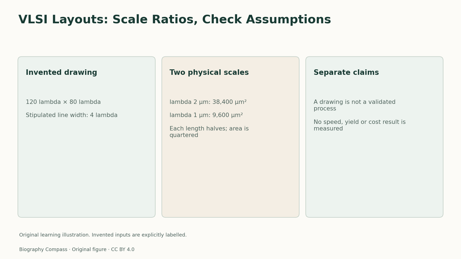
An invented drawing at two scales
Every numerical input is stipulated here.
| Lambda | Rectangle and width rule | Area |
|---|---|---|
| 2 µm | 240 × 160 µm; line 8 µm | 38,400 µm² |
| 1 µm | 120 × 80 µm; line 4 µm | 9,600 µm² |
Chronology
A timeline of the turning points
Participant account
Conway recalls presenting lambda rules.
Teaching
MIT VLSI course.
Representation and access are different changes
Conway’s memoir describes design dimensions as ratios to lambda, a basic length unit. It also calls the initial covering rules crude and non-optimal.
Her retrospective separately describes shared implementation infrastructure and MOSIS.
One record concerns representation; the other concerns getting designs implemented. A rule set can make drawings easier to exchange, but access to a fabrication service also requires coordination, checking and an actual manufacturing process. The two developments reinforce each other without becoming the same event.
Invent a rectangular layout
Take an invented bounding rectangle 120 lambda wide and 80 lambda high. Let lambda first equal 2 µm, then 1 µm. Assume every length scales by the same factor. A separate invented line-width rule is 4 lambda; it is not copied from a historical rule table.
Calculate the two physical rectangles, their areas and the line widths. Then decide whether these answers alone establish that an unchanged circuit can be fabricated on a different process.
Sources for this section: [1]
Reference answer
At 2 µm per lambda, the rectangle is 240 µm by 160 µm and its area is 38,400 µm². At 1 µm per lambda, it is 120 µm by 80 µm and its area is 9,600 µm². Linear dimensions halve; area becomes one quarter. The stipulated line width changes from 8 µm to 4 µm.
The dimensionless drawing is unchanged. Physical length and physical area are not. This arithmetic establishes a geometric transformation under the stated assumption; it does not establish that every device, contact or spacing remains valid. A process-specific check can reject a geometrically neat transformation.
Sources for this section: [1]
What should be compared with the original?
The historical claim is that a ratio-based representation helped make design teachable and reusable. The calculated areas are invented, not measurements of a historical chip. A useful follow-up is to list which assumptions require evidence from outside the drawing: valid process rules, device behaviour, connectivity and fabrication access.
No speed, power, yield or cost improvement follows from the area ratio alone. Those would require their own definitions and measurements. This is why a smaller rectangle is not a complete history of a design methodology.
Continue the chronology
Related history guides
Biography context
Explore United States through connected lives
Connected biographies
A career behind the record
1938–2024
Lynn Conway
Computer engineerChip-design and computer-architecture researcher.Read biographyQuick answers
Common questions
- Is the 4-lambda line rule historical?
- No. It is explicitly invented for the arithmetic.
- Does a quarter-area drawing prove a faster chip?
- No. The model contains no timing, device or interconnect measurements.
Primary and institutional sources
How this history was checked
Selected original records and contextual histories are identified below. Invented examples are teaching models, not reconstructed experiments. This article was reviewed on 31 October 2026.