
The short answer
Why did transistor manufacture need controlled single crystals?
Compare the evidence
Observation, method and result
Compare the inspected records and the different claims they support.
| Record | Evidence | Limit |
|---|---|---|
| CHM grown-junction account | Uniform single crystals and deliberately added impurity regions. | Purity does not mean eliminating all purposeful doping. |
| CHM silicon-transistor account | Separates laboratory success from commercial production. | One working device does not establish a manufacturing supply. |
Uniformity solves one problem
The museum describes a shortage of sufficiently pure, uniform semiconductor material as a major obstacle to junction transistors. Teal’s crystal pulling used a seed withdrawn from molten germanium to obtain a long single crystal. The growth method addresses structure and reproducibility; it does not mean every resulting specimen is identical in all electrical properties. The practical value lies in giving researchers more controlled material on which device ideas can be tested, instead of relying on irregular pieces whose behaviour varies for poorly understood reasons.
Sources for this section: [2]
Doping introduces a useful difference
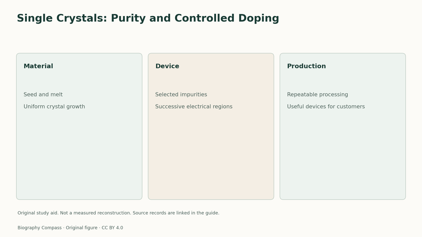
Sparks and Teal added controlled impurities during growth to make successive electrical regions. This is compatible with seeking high purity. Unwanted contamination and deliberate doping are different categories: one introduces uncontrolled variation, while the other is chosen to create a device’s structure. Diagram a seed and melt in one panel, then a simple sequence of labelled regions in another. The drawing should not supply real concentration values or claim that every modern transistor is manufactured by the same early growth procedure.
Sources for this section: [2]
A material advance still needs production
The 1954 record distinguishes Bell’s laboratory silicon transistor from Texas Instruments’ commercial programme. That comparison prevents a single successful demonstration from standing in for a repeatable manufacturing process. A supported answer identifies three separate achievements: obtaining useful material, forming a working device and producing devices for customers. These steps interact, but they are not interchangeable. The guide’s central point is therefore more precise than saying purity makes electronics possible: semiconductor manufacture requires control over which differences are removed and which are deliberately introduced.
Continue the chronology
Related history guides
Biography context
Explore United States through connected lives
Connected biographies
People behind the records
1907–2003
Gordon Teal
Physical chemist and research directorGordon Teal developed single-crystal semiconductor materials and led the Texas Instruments programme that brought silicon transistors into commercial production.Read biography1898–1987
Russell Ohl
Semiconductor researcherRussell Ohl’s investigation of silicon rectifiers revealed a light-sensitive p–n junction that helped establish the foundations of semiconductor devices.Read biographyQuick answers
Common questions
- Why did transistor manufacture need controlled single crystals?
- Uniform single crystals reduce uncontrolled variation. Deliberate impurities can then create the electrical regions needed for a device; purity and controlled doping are compatible goals.
Primary and institutional sources
How this history was checked
Source notes distinguish documented facts from the explanatory examples and diagrams created for this guide. This article was reviewed on 7 November 2026.