
The short answer
Read the historical record, work through the invented example, then identify which conclusions depend on the example’s assumptions.
Read the distinctions
The invented measurements
Compare the kind of statement being made before treating two claims as equivalent.
| Question | First output | Second output |
|---|---|---|
| Voltage gain | 10 | 1 |
| Current gain | 0.5 | 0.5 |
| Power ratio | 5 | 0.5 |
Chronology
A timeline of the turning points
Device history
The museum dates the point-contact work to this month.
Retrospective account
The lecture separates different gains.
The historical sequence matters
Bardeen’s 1956 lecture describes an early gold-contact test that produced some voltage amplification but no power amplification, followed by closely spaced contacts that worked as a point-contact transistor. The record distinguishes that experimental route from the original field-effect proposal.
Brattain’s lecture credits Ohl, Scaff and Theuerer for semiconductor materials. Reading those acknowledgements beside the device account restores the preparation and expertise that a one-person invention story leaves out.
Three ratios answer different questions
The selected device account discusses current, voltage and power amplification separately. That distinction motivates the calculation below; its numbers are invented and are not measurements of the 1947 transistor.
Define this exercise’s average input and output signal powers as P=V×I. The listed voltages and currents are RMS values with voltage and current in phase at each port. No reactive phase correction is needed under that stipulation. A DC supply provides the energy required by the active device; signal gain is not energy creation.
Sources for this section: [1]
Invented measurements
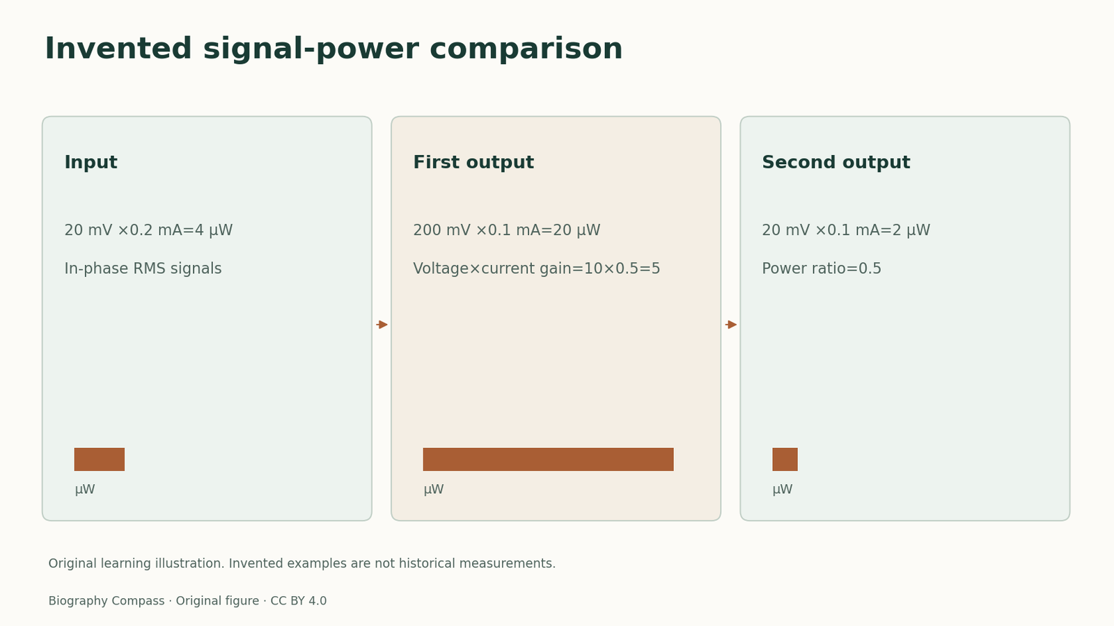
At the input, use 20 mV and 0.2 mA. At the output, use 200 mV and 0.1 mA. Compute voltage gain, current gain, input signal power, output signal power and their power ratio. Does the smaller output current imply that the output signal power must also be smaller? Repeat the power comparison if the output were only 20 mV at the same 0.1 mA.
Write units at every conversion. One millivolt is 0.001 V and one milliampere is 0.001 A. Report powers in microwatts. This fixture asks only about the stated ports and signals; it does not ask for total device efficiency or a safe circuit design.
Sources for this section: [1]
Reference answer and what it establishes
Voltage gain is 200/20=10. Current gain is 0.1/0.2=0.5. Input power is 0.020×0.0002=0.000004 W, or 4 µW. Output power is 0.200×0.0001=0.000020 W, or 20 µW. Power gain is 20/4=5, also 10×0.5. The second output has 2 µW, so its power ratio is 0.5. A current ratio alone settles neither case.
These calculations verify the fixture, not the historical instrument. They do not establish linearity, bandwidth, noise, stability or efficiency. The source-led lesson is that the claimed function of an experiment must match the kind of quantity actually measured.
Sources for this section: [1]
Continue the chronology
Related history guides
Biography context
Explore United States through connected lives
Connected biographies
People behind the records
Quick answers
Common questions
- Is the model an electrical construction guide?
- No. It is arithmetic on stipulated port measurements and omits the information needed to build or assess a real circuit.
Primary and institutional sources
How this history was checked
The cited records have different dates and purposes. All worked examples are newly invented and are not historical measurements. This article was reviewed on 31 October 2026.