
The short answer
How can a junction electrically isolate components on one chip?
Compare the evidence
Observation, method and result
Compare the inspected records and the different claims they support.
| Record | Evidence | Limit |
|---|---|---|
| Lehovec patent | Additional junctions separate regions electrically; 1959 filing/1962 grant. | Does not alone specify every manufacturing step. |
| Physics Today archival research | Places the work within a government-industry-academic career. | A career overview is not a fresh performance test. |
A common slice creates an unwanted connection problem
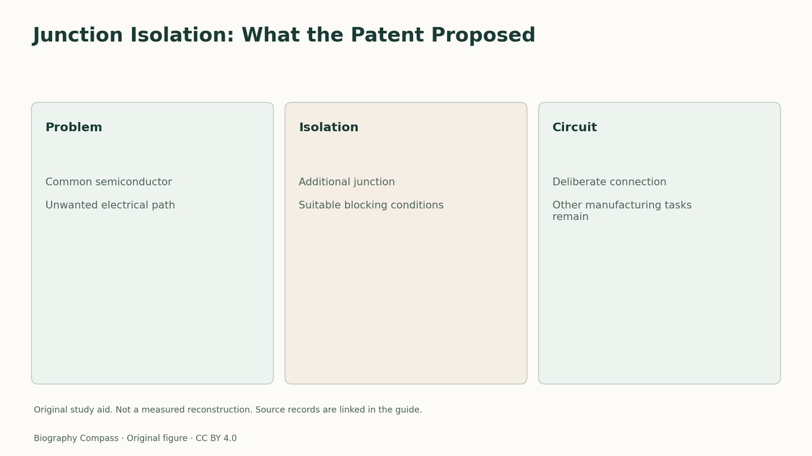
Lehovec’s patent describes several semiconductor components produced on one slice. Sharing material can create electrical paths that are undesirable for the intended circuit. The problem is therefore not only fitting more elements into a small space. Those elements must retain useful electrical distinctions. An original schematic can show two component regions on one substrate, with an unwanted path marked between them. The diagram is an explanation of the issue, not a reproduction of the patent’s geometry or an assertion that every integrated circuit has the same structure.
Sources for this section: [2]
A junction is not an empty gap
The patent proposes arranging additional p–n junctions between component regions. Under suitable blocking conditions, a junction presents high impedance and limits current between them. This is electrical separation within semiconductor material, rather than necessarily sawing the slice into isolated pieces. Intended circuit connections remain a separate design task. Draw a barrier beneath two labelled regions and an authorised connection above. The contrast makes clear that isolation prevents an unwanted path while wiring supplies a wanted one; a useful circuit can require both.
Sources for this section: [2]
Keep chronology and technical scope together
The record dates the application to April 1959 and the grant to April 1962. Physics Today places the work within Lehovec’s Sprague career. A supported answer distinguishes those events rather than reporting a 1959 grant. It also avoids claiming that isolation alone solved packaging, surface reliability, interconnection and production yield. The patent establishes a particular proposal and its claimed scope. The broader importance comes from how electrical separation could support more complex assemblies, while a complete historical account of manufacture requires the related contributions of other people and processes.
Continue the chronology
Related history guides
Biography context
Explore United States through connected lives
Connected biographies
People behind the records
1918–2012
Kurt Lehovec
Physicist and semiconductor researcherKurt Lehovec developed junction-isolation ideas that helped make multiple components on one semiconductor slice electrically workable.Read biography1924–1997
Jean Hoerni
Physicist and semiconductor entrepreneurJean Hoerni developed the planar transistor process and helped build semiconductor companies that extended silicon-device manufacturing.Read biographyQuick answers
Common questions
- How can a junction electrically isolate components on one chip?
- A suitably biased p–n junction limits current between regions on a shared semiconductor slice. It provides electrical separation while deliberate wiring supplies the circuit’s intended connections.
Primary and institutional sources
How this history was checked
Source notes distinguish documented facts from the explanatory examples and diagrams created for this guide. This article was reviewed on 7 November 2026.